Switch timing sequence diagram. Switch-timing diagram for duty cycle 1/3 Time delay circuit diagram timing diagram of circuit switching
Simple Delay Timer Circuits Explained Homemade Circuit, 54% OFF
Switching advantages disadvantages establishment Need timing diagram help Simple delay timer circuits explained – homemade circuit projects
Timer 555 circuit diagram schematic ne555 datasheet discrete kit pinout block does circuits transistor works eleccircuit integrated functional pins connection
Solved complete the timing diagram of the circuit shownBasic timing diagrams for combinational logic circuits 8: timing diagram of the control switch.Time delay circuit diagram.
Delay timer circuits transistor explained timing resistor alarm doorbell schematics electrical sirkuit circuitos discuss keterlambatanTiming diagram of the time switch. Timing diagram of circuit switchingTiming uml logic behavioral.

Provide the timing diagram of the circuits below
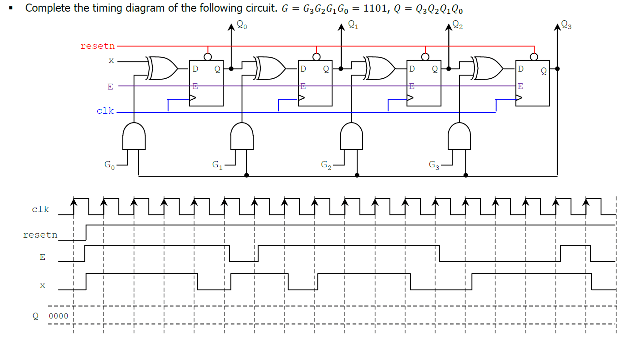
Solved complete the timing diagram of the following circuit.Solved the following circuit and its timing diagram are Example of packet switchingComplete the timing diagram of the circuit shown.
5 second timer circuit diagramSwitching timing diagram Solved complete the timing diagram of the circuit shownTiming diagram of circuit switching.

Timing circuit inspired on time-variant switching phenomena. the figure
How does ne555 timer circuit worksSolved complete the timing diagram of the circuit shown Behavioral uml diagrams : timing diagramDiagram timing circuit complete shown below chegg show.
Solved complete the timing diagram of the following circuit.Solved explain what the circuit is doing and provide a What is circuit switching (circuit-switched network)?Simple delay timer circuits explained homemade circuit, 54% off.

Switch-timing diagram for duty cycle 2/3
Solved which timing diagram below describes this circuitTiming diagrams wisc Timing diagrams (screencast)Solved compare the timing diagram of circuit switching and.
Circuit switchingTiming diagram of circuit switching Solved complete the following timing diagram for the circuit.